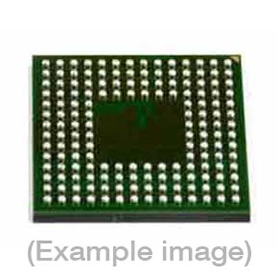
Adapters for Automated Programmers
| 6th Gen | 7th Gen | 9th Gen |
| FXASM72SPB1, FASM72SPB1, FASM72SPB | FX4ASM72SPB1, FXASM72SPB1, FASM72SPB1, FASM72SPB, WX4ASM72SPB1 (repl.) | WX4ASM72SPB1 |
Adapters for Manual Programmers
| 6th Gen | 7th Gen | 9th Gen |
| FXSM72SPB1, FSM72SPB1, FSM72SPB, FXASM72SPB1, FASM72SPB1, FASM72SPB | FX4SM72SPB1, FXSM72SPB1, FSM72SPB1, FSM72SPB, FX4ASM72SPB1, FXASM72SPB1, FASM72SPB1, FASM72SPB, WX4ASM72SPB1 (repl.) | WX4ASM72SPB1 |
Adapters for Engineering Programmers
| 6th Gen | 7th Gen |
| FXSM72SPB1, FSM72SPB1, FSM72SPB, FXASM72SPB1, FASM72SPB1, FASM72SPB | FX4SM72SPB1, FXSM72SPB1, FSM72SPB1, FSM72SPB, FX4ASM72SPB1, FXASM72SPB1, FASM72SPB1, FASM72SPB, WX4ASM72SPB1 (repl.) |
Last Updated: 05/18/2023
If the device is not yet supported by your BPM programmer (Generation), request Device Support
Note
IMPORTANT: Flash Memory with dual 64-bit chip protection registers for security purposes.Please set Default buffer value’ to FFh before loading programming data file.The first 64 bits are programmed at the manufacturing site with a unique 64-bit unchangeable number andwill be read to buffer locations 400000h-400007h. Verify and Compare operations will skipthese locations. The next 64 bits are one time user programmable and mapped at bufferlocations 400008h-40000Fh. The user programmable area protection can be PERMANENTLYenabled under Device/Configure. If the user programmable segment of the protectionregister is not blank or locked device will fail erase. ‘
BPM does not sell programmable devices, nor do we program devices directly. BPM makes programmers and accessories to make programming in-house fast, easy, and profitable.
Additional information
| Manufacturer | SILICON7 |
|---|---|
| Packages | BGA(72) |
| Part Number | SV5C3238UTA |
| Set programming | Yes |
| Vcc(program) | 3 |
| Package |
