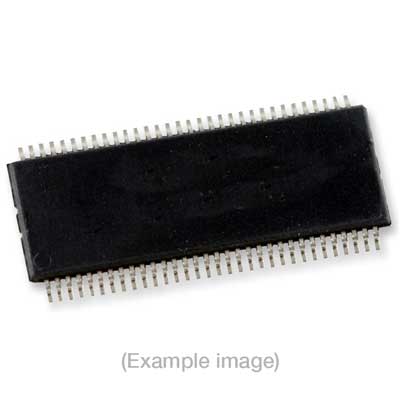
Adapters for Automated Programmers
| 6th Gen | 7th Gen | 9th Gen |
| FXASMR48TD, FXASM48TD, FASMR48TD, FASM48TD, FXASM48TI, FASM48T, FASM56T | FX4ASMR48TD, FX4ASM48TD, FX4ASM48T, FXASMR48TD, FXASM48TD, FASMR48TD, FASM48TD, FXASM48TI, FASM48T, FASM56T, WX4ASMR48TD (repl.), WX4ASM48TD (repl.), WX4ASM48T (repl.) | WX4ASMR48TD, WX4ASM48TD, WX4ASM48T |
Adapters for Manual Programmers
| 6th Gen | 7th Gen | 9th Gen |
| FXSMR48TD, FXSM48TD, FSMR48TD, FSM48TD, FXSM48TI, FSM48T, FSM56TB, FXASMR48TD, FXASM48TD, FASMR48TD, FASM48TD, FXASM48TI, FASM48T, FASM56T, FSM56T (obs.) | FX4SMR48TD, FX4SM48TD, FX4SM48T, FXSMR48TD, FXSM48TD, FSMR48TD, FSM48TD, FXSM48TI, FSM48T, FSM56TB, FX4ASMR48TD, FX4ASM48TD, FX4ASM48T, FXASMR48TD, FXASM48TD, FASMR48TD, FASM48TD, FXASM48TI, FASM48T, FASM56T, FSM56T (obs.), WX4ASMR48TD (repl.), WX4ASM48TD (repl.), WX4ASM48T (repl.) | WX4ASMR48TD, WX4ASM48TD, WX4ASM48T |
Adapters for Engineering Programmers
| 6th Gen | 7th Gen |
| FXSMR48TD, FXSM48TD, FSMR48TD, FSM48TD, FXSM48TI, FSM48T, FSM56TB, FXASMR48TD, FXASM48TD, FASMR48TD, FASM48TD, FXASM48TI, FASM48T, FASM56T, FSM56T (obs.) | FX4SMR48TD, FX4SM48TD, FX4SM48T, FXSMR48TD, FXSM48TD, FSMR48TD, FSM48TD, FXSM48TI, FSM48T, FSM56TB, FX4ASMR48TD, FX4ASM48TD, FX4ASM48T, FXASMR48TD, FXASM48TD, FASMR48TD, FASM48TD, FXASM48TI, FASM48T, FASM56T, FSM56T (obs.), WX4ASMR48TD (repl.), WX4ASM48TD (repl.), WX4ASM48T (repl.) |
Last Updated: 05/18/2023
If the device is not yet supported by your BPM programmer (Generation), request Device Support
Note
IMPORTANT: This is a Flash Memory device with a 128 bit Protection Register. The first 64 bits(located at buffer addresses 200000h-200007h) are pre-programmed by the manufacturer and cannotbe modified. The other 64 bits of the Protection Register (located at buffer addresses 200008h-20000Fh)is OTP programmable. Erasing these bits will return failure if they are not blank.The OTP Data Protection Bit and Security Protection Bit can be set under Device/Configure. Programming these Protection bits is a one-time only operation. If the Security Block Protection Bit is secured the Parameter Block #0 located at [1FE000h-1FFFFFh]in the buffer is no longer erasable or programmable. If the OTP Data Protection Bit is set further programming of the OTP sector of the Protection Register will fail.Setting the OTP Data Protection Bit will also cause further programming of the Security Block Protection Bit to fail.Also please note: If Auto Range Detection’ is set to YES the bits in the Protection Register will not be programmed or verified. ‘
BPM does not sell programmable devices, nor do we program devices directly. BPM makes programmers and accessories to make programming in-house fast, easy, and profitable.
Additional information
| Manufacturer | STMicroelectronics |
|---|---|
| Package | |
| Part Number | M28W160CT85N6 |
| Set programming | Yes |
| Vcc(program) | 3.3 |
| Packages | TSOP(48) |
