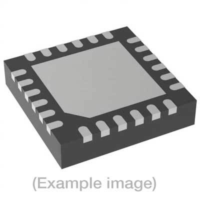
Adapters for Automated Programmers
| 8th Gen | 9th Gen |
| FVE4ASMR48QNP, FVE4ASMR48QNP | FVE4ASMR48QNP |
Adapters for Manual Programmers
| 8th Gen | 9th Gen |
| FVE4ASMR48QNP, FVE4ASMR48QNP | FVE4ASMR48QNP |
Adapters for Engineering Programmers
Last Updated: 05/18/2023
If the device is not yet supported by your BPM programmer (Generation), request Device Support
Note
IMPORTANT:
| Device Type: | MSP430 ultra-low-power FRAM Microcontroller |
| Device Size: | 64KB FRAM code memory + 512B FRAM information memory |
| Algorithm Programming Method: | 4-wire JTAG mode. |
Memory Organization:
| Memory Type |
Attributes(*)
|
Included in default Range (Y/N) | DUT Physical Word Address (hex)(if this area is selected/Activated) | BPWin Buffer Word Address (hex) |
| BSL ROM | R | Yes | 0000_0800 – 0000_0BFF | 0000_0800 – 0000_0BFF |
| FRAM information memory | R/W/E | Yes | 0000_0C00 – 0000_0CFF | 0000_0C00 – 0000_0CFF |
| FRAM code memory | R/W/E | Yes | 0000_2200 – 0000_9FFF | 0000_2200 – 0000_9FFF |
| Default Algorithm Range | — | — | 0000_0C00 – 0000_9FFF | 0000_0C00 – 0000_9FFF |
*R:Read only W: One time programmable (OTP) R/W: readable and one time programmable (OTP) R/W/E: readable and rewritable if not locked. Any configurations listed under Device-Specific’ in the menu item Device-> Settings will be written to the DUT during ‘Program’ operation regardless of memory range selection. Special Device Considerations:
| Word Address | Interrupt Vectors & Signatures Description |
| 7FC0h – 7FFFh | On the FR5xx-6xx devices the physical fuse has been replaced by a programmable electronic fuse. A device can be protected from unauthorized access by restricting accessibility of JTAG commands that can be transferred to the device by the JTAG and SBW interface. This is achieved by programming the electronic fuse. When the device is protected the JTAG and SBW interface still remains functional but JTAG commands that give direct access into the device are completely disabled. There are two ways to lock the device. Both of these require the programming of two signatures that reside in FRAM. JTAG Signature 1 (memory location 0x7FC0) and JTAG Signature 2 (memory location 0x7FC1) control the behavior of the device locking mechanism.Programming invalid data to these locations may prevent further access to the device. |
| 1. | The default device range is set to [0C00h-9FFFh]. This excludes BSL memory. Bootstrap loader(BSL) memory is read only memory. | |
| 2. | Device can be locked by writing 05555h to both JTAG Signature 1 and JTAG Signature 2. | |
| 3. | The only way to unlock the device in this case is to use the BSL to overwrite the JTAG signatures with anything other than 05555h or 0AAAAh. | |
| 4. | This algorithm does not support the BSL programming mode. | |
‘
BPM does not sell programmable devices, nor do we program devices directly. BPM makes programmers and accessories to make programming in-house fast, easy, and profitable.
Additional information
| Manufacturer | Texas Instruments |
|---|---|
| Packages | QFN(48) |
| Part Number | MSP430FR5869IRGZ |
| Vcc(program) | 3 |
| Package |
