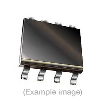
Adapters for Automated Programmers
| 6th Gen | 7th Gen |
| FASMR08SHL, FASM08SHL, FASMR08SHA (obs.), FASM08SHA (obs.), FASM08SH (obs.) | FASMR08SHL, FASM08SHL, FASMR08SHA (obs.), FASM08SHA (obs.), FASM08SH (obs.) |
Adapters for Manual Programmers
| 6th Gen | 7th Gen | 9th Gen |
| FSMR08SHL, FSM08SHL, FASMR08SHL, FASM08SHL, FSMR08SHA (obs.), FSM08SHA (obs.), FSM08SH (obs.), FASMR08SHA (obs.), FASM08SHA (obs.), FASM08SH (obs.), WX4ASMR08SHA (obs.) (repl.), LX4ASM08SHL (repl.), WASM08SH (obs.) (repl.), WASM08SHA (obs.) (repl.) | FSMR08SHL, FSM08SHL, FASMR08SHL, FASM08SHL, FSMR08SHA (obs.), FSM08SHA (obs.), FSM08SH (obs.), FASMR08SHA (obs.), FASM08SHA (obs.), FASM08SH (obs.), WX4ASMR08SHA (obs.) (repl.), LX4ASM08SHL (repl.), WASM08SH (obs.) (repl.), WASM08SHA (obs.) (repl.) | WX4ASMR08SHA (obs.), LX4ASM08SHL, WX4ASM08SHB (obs.), WASM08SH (obs.), WASM08SHA (obs.) |
Adapters for Engineering Programmers
| 6th Gen | 7th Gen |
| FSMR08SHL, FSM08SHL, FASMR08SHL, FASM08SHL, FSMR08SHA (obs.), FSM08SHA (obs.), FSM08SH (obs.), FASMR08SHA (obs.), FASM08SHA (obs.), FASM08SH (obs.), WX4ASMR08SHA (obs.) (repl.), LX4ASM08SHL (repl.), WASM08SH (obs.) (repl.), WASM08SHA (obs.) (repl.) | FSMR08SHL, FSM08SHL, FASMR08SHL, FASM08SHL, FSMR08SHA (obs.), FSM08SHA (obs.), FSM08SH (obs.), FASMR08SHA (obs.), FASM08SHA (obs.), FASM08SH (obs.), WX4ASMR08SHA (obs.) (repl.), LX4ASM08SHL (repl.), WASM08SH (obs.) (repl.), WASM08SHA (obs.) (repl.) |
Last Updated: 05/18/2023
If the device is not yet supported by your BPM programmer (Generation), request Device Support
Note
IMPORTANT: Microcontroller with FLASH.The following describes the Buffer setup.The addresses [$F800-$FDFF] [$FFB0-$FFBD] and [$FFC2-$FFCF] are Flash.The addresses [$FFD0-$FFFF] are Flash User Vectors.The address [$FFBE] is FLASH Block Protection Register(FLBPR).This device has an eight byte security feature from $FFF6 to $FFFD. To Read or Verify aprogrammed device the buffer or Device Configure must be filled with correct data fromaddress $FFF6 to $FFFD. Incorrect data at these locations will prevent access to the device.*** During Erase factory programmed trim value at addresses $FFC0 and $FFC1 will be saved first and restoredat the end. Erase operation uses the Erase Passwords in Device Configure to read the factory trimvalue. Erase will fail if the Erase Passwords do not match the device. A blank devicecan use all $FF’s for the Erase Passwords.ID Check actually reads the factory trim value.The ID Check cannot be disabled.During Verify the factory trim value is read back and verified against the stored value during ID Check.The Verify after programming’ must not be disabled. ‘
BPM does not sell programmable devices, nor do we program devices directly. BPM makes programmers and accessories to make programming in-house fast, easy, and profitable.
Additional information
| Manufacturer | Freescale Semiconductor |
|---|---|
| Packages | SOIC(8) |
| Part Number | MC68HC908QT1CDWE |
| Vcc(program) | 5 |
| 8-bit Bytes | |
| Package |
