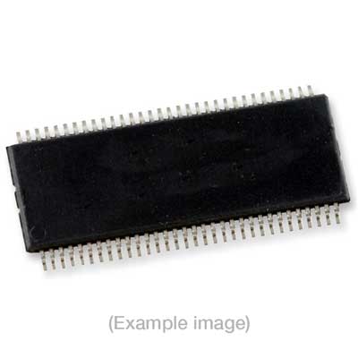
Adapters for Automated Programmers
| 6th Gen | 7th Gen | 8th Gen | 9th Gen | Flashstream |
| FXASMR48TD, FXASM48TD, FASMR48TD, FASM48TD, FXASM48TA, FASM48T, FASM56T | FX4ASMR48TD, FX4ASM48TD, FX4ASM48T, FXASMR48TD, FXASM48TD, FASMR48TD, FASM48TD, FXASM48TA, FASM48T, FASM56T | FVE4ASMR48TSL, FVE4ASMR48TS, FVE4ASM48TS, FVE4ASMR48TSL, FVE4ASMR48TS, FVE4ASM48TS | FVE4ASMR48TSL, FVE4ASMR48TS, FVE4ASM48TS | FVE4ASMR48TSL, FVE4ASMR48TS, FVE4ASM48TS, FVE4ASMR48TSL, FVE4ASMR48TS, FVE4ASM48TS |
Adapters for Manual Programmers
| 6th Gen | 7th Gen | 8th Gen | 9th Gen | Flashstream |
| FXSMR48TD, FXSM48TD, FSMR48TD, FSM48TD, FXSM48TA, FSM48T, FSM56TB, FXASMR48TD, FXASM48TD, FASMR48TD, FASM48TD, FXASM48TA, FASM48T, FASM56T, FSM56T (obs.) | FX4SMR48TD, FX4SM48TD, FX4SM48T, FXSMR48TD, FXSM48TD, FSMR48TD, FSM48TD, FXSM48TA, FSM48T, FSM56TB, FX4ASMR48TD, FX4ASM48TD, FX4ASM48T, FXASMR48TD, FXASM48TD, FASMR48TD, FASM48TD, FXASM48TA, FASM48T, FASM56T, FSM56T (obs.), WX4ASMR48TD (repl.), WX4ASM48TD (repl.), WX4ASM48T (repl.) | FVE4ASMR48TSL, FVE4ASMR48TS, FVE4ASM48TS, FVE4ASMR48TSL, FVE4ASMR48TS, FVE4ASM48TS | FVE4ASMR48TSL, FVE4ASMR48TS, FVE4ASM48TS | FVE4ASMR48TSL, FVE4ASMR48TS, FVE4ASM48TS, FVE4ASMR48TSL, FVE4ASMR48TS, FVE4ASM48TS |
Adapters for Engineering Programmers
| 6th Gen | 7th Gen |
| FXSMR48TD, FXSM48TD, FSMR48TD, FSM48TD, FXSM48TA, FSM48T, FSM56TB, FXASMR48TD, FXASM48TD, FASMR48TD, FASM48TD, FXASM48TA, FASM48T, FASM56T, FSM56T (obs.) | FX4SMR48TD, FX4SM48TD, FX4SM48T, FXSMR48TD, FXSM48TD, FSMR48TD, FSM48TD, FXSM48TA, FSM48T, FSM56TB, FX4ASMR48TD, FX4ASM48TD, FX4ASM48T, FXASMR48TD, FXASM48TD, FASMR48TD, FASM48TD, FXASM48TA, FASM48T, FASM56T, FSM56T (obs.), WX4ASMR48TD (repl.), WX4ASM48TD (repl.), WX4ASM48T (repl.) |
Last Updated: 05/18/2023
If the device is not yet supported by your BPM programmer (Generation), request Device Support
Note
IMPORTANT: 16-megabit Flash Memory with 128 bit Protection Register.The first 64 bits Block A (located at buffer addresses 200000h-200007h) are pre-programmed at the factory.These bits cannot be modified and are ignored during Compare and Verify.The second 64 bits Block B are user programmable and they arelocated at buffer locations 200008h-20000Fh.Locking the Block B of the Protection Register is a one time only operation.If the Block B is programmed or locked chip erase will fail.Please refer to device specifications for more information.The default Device Range is set to [00000h-FFFFFh].Please select Entire File’ under Device Range if Extended Memory Block need to be included. ‘
BPM does not sell programmable devices, nor do we program devices directly. BPM makes programmers and accessories to make programming in-house fast, easy, and profitable.
Additional information
| Manufacturer | Atmel |
|---|---|
| Package | |
| Packages | TSOP(48) |
| Bytes | 0h-F 7FFFh; F 8000h-F FFFFh; 10 0000h-10 0003h; 10 0004h-10 0007h |
| ByteWidth | AT49BV162AT-70TU (ID=C2h) |
| VccProgram | 16-bit words |
| VppProgram | 1048584 |
| ElectricalErase | 3 |
