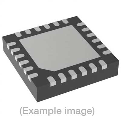
Adapters for Automated Programmers
| 8th Gen |
| FVE4ASMR40QFNWB, FVE4ASMR40QFNWB |
Adapters for Manual Programmers
| 8th Gen |
| FVE4ASMR40QFNWB, FVE4ASMR40QFNWB |
Adapters for Engineering Programmers
Last Updated: 05/18/2023
If the device is not yet supported by your BPM programmer (Generation), request Device Support
Note
IMPORTANT:
| Device Type: | 32-bit ARM Cortex-M0 Microcontroller |
| Device Size: | 128 KB Flash |
Memory Organization:
| Memory Type |
Attributes(*)
|
Included in default Range (Y/N) | DUT Physical Byte Address(hex)(if this area is selected/Activated) | BPWin Buffer Byte Address(hex) |
| User’s Flash | R/W/E | Yes | 0000_0000 – 0001_FFFF | 0000_0000 – 0001_FFFF |
| Checksum | R | Yes | 9030_0000 – 9030_0001 | 9030_0000 – 9030_0001 |
| Flash Protection (of user’s row) | R/W/E | Yes | 9040_0000 – 9040_003F | 9040_0000 – 9040_003F |
| Meta Data | R | Yes | 9050_0000 – 9050_000B | 9050_0000 – 9050_000B |
| Chip Level Protection | R/W/E | Yes | 9060_0000 – 9060_0000 | 9060_0000 – 9060_0000 |
| Default Algorithm Range | — | — | 0000_0000 – 9060_0000 | 0000_0000 – 9060_0000 |
* R:Read only W: One time programmable (OTP) R/W: readable and one time programmable (OTP) R/W/E: readable and rewritable if not locked. Any configurations listed under Device-Specific’ in the menu item Device-> Settings will be written to the DUT during ‘Program’ operation regardless of memory range selection. Special Device Considerations:
| 1. | Serialization is not supported. | |
| 2. | Meta Data [9050_0000h – 9050_000Bh] is used to check the integrity of the hex file and the silicon ID of the target device. | |
| Only data at address 9050_0002h 9050_0003h and 9050_0004h are read. All other data in this section are ignored. | ||
| If the data file ID does not match the ID of the target device PROGRAM will fail. | ||
| 3. | Chip Level Protection [9060_0000h] has four states: | |
| – VIRGIN(0x00):In this mode the silicon is in post-fab (untrimmed state). This mode is not for custom use. | ||
| – OPEN(0x01):In this mode Flash STRAM supervisory flash and registers can be accessed via the DAP. | ||
| – PROTECTED(0x02): In this mode access to Flash SRAM and most registers are disabled. Can Erase and reprogram Flash. | ||
| – KILL(0x04): In this mode device locks SWD-pins from external programmer. All operations will fail if device is in this mode. | ||
‘
BPM does not sell programmable devices, nor do we program devices directly. BPM makes programmers and accessories to make programming in-house fast, easy, and profitable.
Additional information
| Manufacturer | Cypress |
|---|---|
| Packages | LAP(40) |
| Part Number | CYPD4226-40LQXIT |
| Set programming | Yes |
| Vcc(program) | 3.3 |
| 8-bit Bytes | |
| Package |
