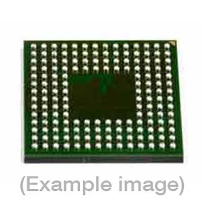
Adapters for Automated Programmers
| 8th Gen | 9th Gen | Flashstream |
| FVE4ASMC24BGJ, FVE4ASM24BGB, FVE4ASMC24BGJ, FVE4ASM24BGB | FVE4ASMC24BGJ, FVE4ASM24BGB | FVE4ASMC24BGJ, FVE4ASM24BGB, FVE4ASMC24BGJ, FVE4ASM24BGB |
Adapters for Manual Programmers
| 8th Gen | 9th Gen | Flashstream |
| FVE4ASMC24BGJ, FVE4ASM24BGB, FVE4ASMC24BGJ, FVE4ASM24BGB | FVE4ASMC24BGJ, FVE4ASM24BGB | FVE4ASMC24BGJ, FVE4ASM24BGB, FVE4ASMC24BGJ, FVE4ASM24BGB |
Adapters for Engineering Programmers
Last Updated: 05/18/2023
If the device is not yet supported by your BPM programmer (Generation), request Device Support
Note
IMPORTANT: 1 Gigabit MirrorBit Flash memory. Dual Die Stack of two FS512S die. This algorithm uses Standard SPI mode to Program and Verify/Read the device. The status register bits can be set under Device Config > Configure . The default Device Range is set to [0000000h-7FFFFFFh]. Please modify the range under Device Config > Range if any of the Security Registers need to be included. The OTP region is located in the range [8000000h-80003FFh]. The Factory Programmed 128-bit random number located at the beginning of the OTP region cannot be programmed and data in this region will not be shown in the Buffer Editor. OTP Lock bits are located in the Buffer location [8000010h-8000013h] and Reserved bits are located at [8000014h-800001Fh].
BPM does not sell programmable devices, nor do we program devices directly. BPM makes programmers and accessories to make programming in-house fast, easy, and profitable.
Additional information
| Manufacturer | Cypress |
|---|---|
| Packages | BGA(24) |
| Part Number | S70FS01GSDSBHM21 |
| Set programming | Yes |
| Vcc(program) | 1.9 |
| 8-bit Bytes | |
| Package |
