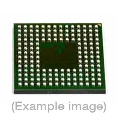
Adapters for Automated Programmers
| 6th Gen | 7th Gen | 9th Gen |
| FASMR100BGZ | FX4ASMR100BGZ, FASMR100BGZ, LX4ASMR100BGZ (repl.) | LX4ASMR100BGZ |
Adapters for Manual Programmers
| 6th Gen | 7th Gen | 9th Gen |
| FASMR100BGZ | FX4ASMR100BGZ, FASMR100BGZ, LX4ASMR100BGZ (repl.) | LX4ASMR100BGZ |
Adapters for Engineering Programmers
| 6th Gen | 7th Gen |
| FASMR100BGZ | FX4ASMR100BGZ, FASMR100BGZ, LX4ASMR100BGZ (repl.) |
Last Updated: 05/18/2023
If the device is not yet supported by your BPM programmer (Generation), request Device Support
Note
IMPORTANT:
| Device Type: | Microcontroller |
| Device Size: | 2MB flash |
| Algorithm Programming Method: | Jtag + Nexus mode |
Memory Organization:
| Memory Type |
Attributes(*)
|
Included in default Range (Y/N) | DUT Physical Byte Address(hex)(if this area is selected/Activated) | BPWin Buffer Byte Address(hex) | UTEST (DCF+ OTP-12228 Bytes). | R/W | No | 0020 0270 – 0020 1FFF | 0040 04E0 – 0040 3FFF |
| 128KB HSM code space. | R/W/E | Yes | 0030 8000 – 0031 7FFF | 0061 0000 – 0062 FFFF |
| 32KB HSM data space. | R/W/E | Yes | 007C 0000 – 007C 3FFF | 00F8 0000 – 00F8 7FFF |
| (16KB+128KB) Small HSM Code Block + Small and Medium NVM Block space. | R/W/E | Yes | 007C 6000 – 007D 7FFF | 00F8 C000 – 00FA FFFF |
| 256KB Small & Medium NVM Blocks space. | R/W/E | Yes | 007E 0000 – 007F FFFF | 00FC 0000 – 00FF FFFF | 2560KB Large Flash NVM. | R/W/E | Yes | 0080 0000 – 0093 FFFF | 0100 0000 – 0127 FFFF |
| Default Algorithm Range | — | — | 0030 8000 – 0093 FFFF | 0061 0000 – 0127 FFFF |
* R:Read only W: One time programmable (OTP) R/W: readable and one time programmable (OTP) R/W/E: readable and rewritable if not locked. Any configurations listed under Device-Specific’ in the menu item Device-> Settings will be written to the DUT during ‘Program’ operation. Special Device Considerations: After a successful Program + Verify operation subsequent stand alone operations may fail if the Customer Data Pattern code executes to modify the Code Flash. The default Device Range is set to Flash Memory map [308000h-93FFFFh] which is mapped to Data Pattern byte address [610000h-127FFFFh]. Please select Entire Device under Device Config if DCF Records and Customer OTP need to be included. Verify command can fail after programming DCF Record since the customer code may execute after being programmed. ‘
BPM does not sell programmable devices, nor do we program devices directly. BPM makes programmers and accessories to make programming in-house fast, easy, and profitable.
Additional information
| Manufacturer | Freescale Semiconductor |
|---|---|
| Packages | TEPBGA(100) |
| Part Number | SC667551MMH2R |
| Set programming | Yes |
| Vcc(program) | 1.2 |
| Package |
