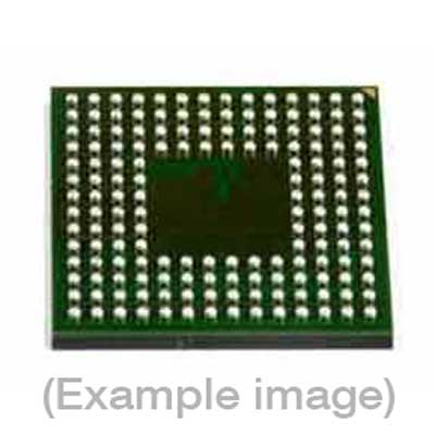
Adapters for Automated Programmers
| 8th Gen | 9th Gen |
| FVE2ASMR292LFBGC, FVE2ASMR292LFBGC | FVE2ASMR292LFBGC |
Adapters for Manual Programmers
| 8th Gen | 9th Gen |
| FVE2ASMR292LFBGC, FVE2ASMR292LFBGC | FVE2ASMR292LFBGC |
Adapters for Engineering Programmers
Last Updated: 05/18/2023
If the device is not yet supported by your BPM programmer (Generation), request Device Support
Note
IMPORTANT:
| Device Type: | AURIX 32-Bit Single-Chip Microcontroller |
| Device Size: | 8 MByte PFlash Memory + 768 Kbytes DFlash Memory |
| Algorithm Programming Method: | DAP |
Memory Organization:
| Memory Type |
Attributes(*)
|
Included in default Range (Y/N) | DUT Physical Byte Address(hex)(if this area is selected/Activated) | BPWin Buffer Byte Address(hex) |
| PFlash0 | R/W/E | Yes | A000_0000 – A01F_FFFF | 0000_0000 – 0027_FFFF | PFlash1 | R/W/E | Yes | A020_0000 – A03F_FFFF | 0028_0000 – 004F_FFFF | PFlash2 | R/W/E | Yes | A040_0000 – A05F_FFFF | 0050_0000 – 0077_FFFF | PFlash3 | R/W/E | Yes | A060_0000 – A07F_FFFF | 0078_0000 – 009F_FFFF | DFlash0 DF_EEPROM | R/W/E | Yes | AF00_0000 – AF0B_FFFF | 00A0_0000 – 00AE_FFFF |
| DFlash0 DF_UCB | R/W/E | No | AF10_0000 – AF10_1BFF | 00AF_0000 – 00AF_22FF |
| Default Algorithm Range | — | — | A000_0000 – AF0B_FFFF | 0000_0000 – 00AE_FFFF |
* R:Read only W: One time programmable (OTP) R/W: readable and one time programmable (OTP) R/W/E: readable and rewritable if not locked. Any configurations listed under Device-Specific’ in the menu item Device-> Settings will be written to the DUT during ‘Program’ operation regardless of memory range selection. Special Device Considerations:
| 1. | This device selection requires a data file formatted using the image format tool under Device->Image_Format.Alternatively Read will also return the data from a programmed sample in the correct format.Please contact BP Microsystems for information on how to use the image format tool. |
| 2. | This device selection requires the FVE2ASMR292LFBGC socket module.To use the FVE2ASMR292LFBGB socket module please use the SAK-TC297TP-128F300S BB QSor SAK-TC297TX-128F300S BB QS device selection. |
| 3. | This algorithm only supports UCB0-UCB6. UCB2 and UCB3 are OTP. UCB4 is factory set and is not programmable.If a given UCB does not have data in the Data Buffer it will be skipped during all operations.The UCBs are erased prior to programming them during the Program operation not in the Erase operation. |
| 4. | When reading a blank logical sector there may be bit errors due to unprogrammed ECC.Thus it is recommended to program the entire PFlash and DFlash (DF_EEPROM). |
| 5. | Simple serialization is not supported. |
‘
BPM does not sell programmable devices, nor do we program devices directly. BPM makes programmers and accessories to make programming in-house fast, easy, and profitable.
Additional information
| 8-bit Bytes | 11477760 |
|---|---|
| Manufacturer | Infineon(Siemens) |
| Packages | LFBGA(292) |
| Part Number | SAK-TC297TX-128F300S |
| Vcc(program) | 1.3 |
| Package |
