Adapters for Automated Programmers
| 6th Gen | 7th Gen | 8th Gen | 9th Gen | Flashstream |
| FXASMR64EBGF, FXASM64EBGF, FXASM64EBGE, FASMR64EBGF, FASM64EBGF, FASM64EBGE, FXASM64EBGC, FXASM64EBGA, FASM64EBGC | FX4ASMR64EBGF, FX4ASM64EBGF, FX4ASM64EBGE, FXASMR64EBGF, FXASM64EBGF, FXASM64EBGE, FASMR64EBGF, FASM64EBGF, FASM64EBGE, FXASM64EBGC, FXASM64EBGA, FASM64EBGC | FVE4ASM64EBGF, FVE4ASM64EBGF | FVE4ASM64EBGF | FVE4ASM64EBGF, FVE4ASM64EBGF |
Adapters for Manual Programmers
| 6th Gen | 7th Gen | 8th Gen | 9th Gen | Flashstream |
| FXSMR64EBGF, FXSM64EBGF, FXSM64EBGE, FSMR64EBGF, FSM64EBGF, FSM64EBGE, FXSM64EBGC, FXSM64EBGA, FSM64EBGC, FXASMR64EBGF, FXASM64EBGF, FXASM64EBGE, FASMR64EBGF, FASM64EBGF, FASM64EBGE, FXASM64EBGC, FXASM64EBGA, FASM64EBGC | FX4SMR64EBGF, FX4SM64EBGF, FX4SM64EBGE, FXSMR64EBGF, FXSM64EBGF, FXSM64EBGE, FSMR64EBGF, FSM64EBGF, FSM64EBGE, FXSM64EBGC, FXSM64EBGA, FSM64EBGC, FX4ASMR64EBGF, FX4ASM64EBGF, FX4ASM64EBGE, FXASMR64EBGF, FXASM64EBGF, FXASM64EBGE, FASMR64EBGF, FASM64EBGF, FASM64EBGE, FXASM64EBGC, FXASM64EBGA, FASM64EBGC, WX4ASM64EBGF (repl.), LX4ASMR64EBGF (repl.), WX4ASM64EBGE (repl.) | FVE4ASM64EBGF, FVE4ASM64EBGF | FVE4ASM64EBGF | FVE4ASM64EBGF, FVE4ASM64EBGF |
Adapters for Engineering Programmers
| 6th Gen | 7th Gen |
| FXSMR64EBGF, FXSM64EBGF, FXSM64EBGE, FSMR64EBGF, FSM64EBGF, FSM64EBGE, FXSM64EBGC, FXSM64EBGA, FSM64EBGC, FXASMR64EBGF, FXASM64EBGF, FXASM64EBGE, FASMR64EBGF, FASM64EBGF, FASM64EBGE, FXASM64EBGC, FXASM64EBGA, FASM64EBGC | FX4SMR64EBGF, FX4SM64EBGF, FX4SM64EBGE, FXSMR64EBGF, FXSM64EBGF, FXSM64EBGE, FSMR64EBGF, FSM64EBGF, FSM64EBGE, FXSM64EBGC, FXSM64EBGA, FSM64EBGC, FX4ASMR64EBGF, FX4ASM64EBGF, FX4ASM64EBGE, FXASMR64EBGF, FXASM64EBGF, FXASM64EBGE, FASMR64EBGF, FASM64EBGF, FASM64EBGE, FXASM64EBGC, FXASM64EBGA, FASM64EBGC, WX4ASM64EBGF (repl.), LX4ASMR64EBGF (repl.), WX4ASM64EBGE (repl.) |
Last Updated: 05/18/2023
If the device is not yet supported by your BPM programmer (Generation), request Device Support
Note
IMPORTANT: This device contains 128 bit Protection Register. The first 64 bits are mappedfrom 2000000h to 2000007h in the buffer. These bits are pre-programmed by themanufacturer and cannot be modified. The last 64 bits of theProtection Register are mapped from 2000008h to 200000Fh in the buffer and areone-time-user-programmable. When erasing Protection Register and OBLAthe programmer will blank-check these bits and will fail erase if theyare not blank. Locking the user-programmable segment of theProtection Register is a one time only operation. The Erasable Block Lock-bit Array(EBLA)Block Locking Configuration Register(BLCR) and OTP Block Lock-bit Array(OBLA) can be set in Device Configure.To use the OBLA for permanent block locking bit 7 of BLCR must be set to 0otherwise OBLA will be skipped during program and may fail verify.If certain bits of BLCR are programmed to 0 the Erasable Block Lock-Bit Array(EBLA)and/or OBLA may not be programmed any more. This algorithm will reject a part if bit 0 bit 2 bit 6 or bit 7 of BLCR is not blank. It’s suggested that the BLCR value is knownto the user before programming.The default Device Range is set to [000000h-FFFFFFh]. Please select Entire File’ under Device Range if Protection Registers need to be included. ‘
BPM does not sell programmable devices, nor do we program devices directly. BPM makes programmers and accessories to make programming in-house fast, easy, and profitable.
Additional information
| Manufacturer | Intel |
|---|---|
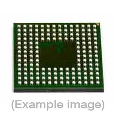
| Packages | BGA(64) |
| Part Number | PC28F256J3D95 |
| Set programming | Yes |
| Vcc(program) | 3.3 |
| Package |
