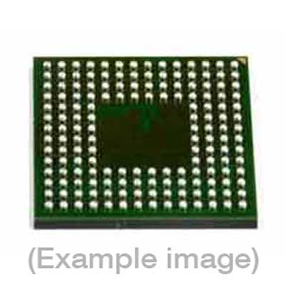
Adapters for Automated Programmers
| 6th Gen | 7th Gen | 8th Gen | 9th Gen | Flashstream |
| FXASM64LBGA, FASM64LBGA, FXASM64FBGA (obs.), FASM64FBGA (obs.), FXASM64FBGB (obs.), FASM64FBGB (obs.) | FX4ASM64LBGA, FXASM64LBGA, FASM64LBGA, FXASM64FBGA (obs.), FASM64FBGA (obs.), FX4ASM64FBGB (obs.), FXASM64FBGB (obs.), FASM64FBGB (obs.) | FVE4ASMR64LBGA, FVE4ASM64LBGA, FVE4ASM64FBGB (obs.), FVE4ASM64LBGA, FVE4ASM64FBGB (obs.), FVE4ASMR64LBGA | FVE4ASM64LBGA, FVE4ASM64FBGB (obs.), FVE4ASMR64LBGA | FVE4ASMR64LBGA, FVE4ASM64LBGA, FVE4ASM64FBGB (obs.), FVE4ASM64LBGA, FVE4ASM64FBGB (obs.), FVE4ASMR64LBGA |
Adapters for Manual Programmers
| 6th Gen | 7th Gen | 8th Gen | 9th Gen | Flashstream |
| FXSM64LBGA, FSM64LBGA, FXASM64LBGA, FASM64LBGA, FXSM64FBGA (obs.), FSM64FBGA (obs.), FXASM64FBGA (obs.), FASM64FBGA (obs.), FXSM64FBGB (obs.), FSM64FBGB (obs.), FXASM64FBGB (obs.), FASM64FBGB (obs.) | FX4SM64LBGA, FXSM64LBGA, FSM64LBGA, FX4ASM64LBGA, FXASM64LBGA, FASM64LBGA, FXSM64FBGA (obs.), FSM64FBGA (obs.), FXASM64FBGA (obs.), FASM64FBGA (obs.), FX4SM64FBGB (obs.), FXSM64FBGB (obs.), FSM64FBGB (obs.), FX4ASM64FBGB (obs.), FXASM64FBGB (obs.), FASM64FBGB (obs.), WX4ASM64FBGB (obs.) (repl.), LX4ASM64LBGA (repl.) | FVE4ASMR64LBGA, FVE4ASM64LBGA, FVE4ASM64FBGB (obs.), FVE4ASM64LBGA, FVE4ASM64FBGB (obs.), FVE4ASMR64LBGA | FVE4ASM64LBGA, FVE4ASM64FBGB (obs.), FVE4ASMR64LBGA | FVE4ASMR64LBGA, FVE4ASM64LBGA, FVE4ASM64FBGB (obs.), FVE4ASM64LBGA, FVE4ASM64FBGB (obs.), FVE4ASMR64LBGA |
Adapters for Engineering Programmers
| 6th Gen | 7th Gen |
| FXSM64LBGA, FSM64LBGA, FXASM64LBGA, FASM64LBGA, FXSM64FBGA (obs.), FSM64FBGA (obs.), FXASM64FBGA (obs.), FASM64FBGA (obs.), FXSM64FBGB (obs.), FSM64FBGB (obs.), FXASM64FBGB (obs.), FASM64FBGB (obs.) | FX4SM64LBGA, FXSM64LBGA, FSM64LBGA, FX4ASM64LBGA, FXASM64LBGA, FASM64LBGA, FXSM64FBGA (obs.), FSM64FBGA (obs.), FXASM64FBGA (obs.), FASM64FBGA (obs.), FX4SM64FBGB (obs.), FXSM64FBGB (obs.), FSM64FBGB (obs.), FX4ASM64FBGB (obs.), FXASM64FBGB (obs.), FASM64FBGB (obs.), WX4ASM64FBGB (obs.) (repl.), LX4ASM64LBGA (repl.) |
Last Updated: 05/18/2023
If the device is not yet supported by your BPM programmer (Generation), request Device Support
Note
IMPORTANT: This is a Flash Memory with an additional Security Sector (OTP). This sector is mapped from 4000000h to 4000007Fh (Data Pattern locations: 8000000h – 80000FFh). This sector can be purchased programmed and locked from the factory. If this is the case this sector needs to be excluded from programming and verification ranges as this data could have a unique number. The configuration option for the factory lock is used to indicate the status of the chip. If this option is different than the state of the chip during verification or compare it will cause an error. If the part has not been locked by the factory the user can treat this sector as an additional memory sector with OTP sector protection. The 4-Word Password area is mapped from 4000080h-4000083h (Data Pattern locations: 8000100h-8000107h). Once Password Protection Mode Lock bit is set protected sector groups can no longer be unprotected by this algorithm. Password area is only verified right after it is programmed with Program operation. The default Device Range is set to [000000h-3FFFFFFh]. Please select Entire File’ under Device Range if Security sector needs to be included. ‘
BPM does not sell programmable devices, nor do we program devices directly. BPM makes programmers and accessories to make programming in-house fast, easy, and profitable.
Additional information
| Manufacturer | Macronix |
|---|---|
| Packages | BGA(64) |
| Part Number | MX68GL1G0FDXFI-11G |
| Set programming | Yes |
| Vcc(program) | 3.3 |
| Package |
