Adapters for Automated Programmers
| 6th Gen | 7th Gen | 9th Gen |
| FXASM77BGA, FASM77BGA | FX4ASM77BGA, FXASM77BGA, FASM77BGA, WX4ASM77BGA (repl.) | WX4ASM77BGA |
Adapters for Manual Programmers
| 6th Gen | 7th Gen | 9th Gen |
| FXSM77BGA, FSM77BGA, FXASM77BGA, FASM77BGA | FX4SM77BGA, FXSM77BGA, FSM77BGA, FX4ASM77BGA, FXASM77BGA, FASM77BGA, WX4ASM77BGA (repl.) | WX4ASM77BGA |
Adapters for Engineering Programmers
| 6th Gen | 7th Gen |
| FXSM77BGA, FSM77BGA, FXASM77BGA, FASM77BGA | FX4SM77BGA, FXSM77BGA, FSM77BGA, FX4ASM77BGA, FXASM77BGA, FASM77BGA, WX4ASM77BGA (repl.) |
Last Updated: 05/18/2023
If the device is not yet supported by your BPM programmer (Generation), request Device Support
Note
IMPORTANT: This device contains two MT28F644W18T Flashes. In the buffer addresses 000000h-7FFFFFh are forFlash 1 addresses 800000h-FFFFFFh are for Flash 2.Each MT28F644W18T has 128-bit Protection Register. The first 64 bits are pre-programmedby the manufacturer and cannot be modified while the other 64 bits are one-time user programmable.The 128 bits Protection Register of Flash 1 are located at buffer addresses 1000000h-100000Fh.The 128 bits Protection Register of Flash 2 are located at buffer addresses 1000010h-100001Fh.The OTP area protection can be PERMANENTLY enabled under Device/Configure.If the user programmable segment of the Protection Register is not blank or lockedthe Protection Register ranges must be excluded in erase/program range.
BPM does not sell programmable devices, nor do we program devices directly. BPM makes programmers and accessories to make programming in-house fast, easy, and profitable.
Additional information
| Manufacturer | Micron |
|---|---|
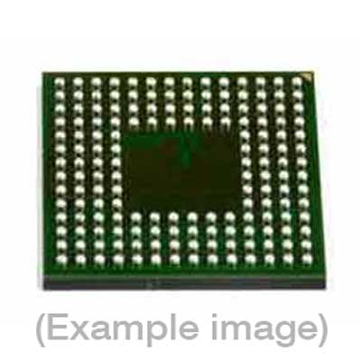
| Packages | BGA(77) |
| Part Number | MT28C128532W18DFW-TT |
| Set programming | Yes |
| Vcc(program) | 1.8 |
| Package |
