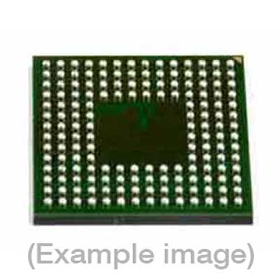
Adapters for Automated Programmers
| 6th Gen | 7th Gen | 9th Gen |
| FXASM88BGB, FASM88BGB | FX4ASM88BGB, FXASM88BGB, FASM88BGB, WX4ASM88BGB (repl.) | WX4ASM88BGB |
Adapters for Manual Programmers
| 6th Gen | 7th Gen | 9th Gen |
| FXSM88BGB, FSM88BGB, FXASM88BGB, FASM88BGB | FX4SM88BGB, FXSM88BGB, FSM88BGB, FX4ASM88BGB, FXASM88BGB, FASM88BGB, WX4ASM88BGB (repl.) | WX4ASM88BGB |
Adapters for Engineering Programmers
| 6th Gen | 7th Gen |
| FXSM88BGB, FSM88BGB, FXASM88BGB, FASM88BGB | FX4SM88BGB, FXSM88BGB, FSM88BGB, FX4ASM88BGB, FXASM88BGB, FASM88BGB, WX4ASM88BGB (repl.) |
Last Updated: 05/18/2023
If the device is not yet supported by your BPM programmer (Generation), request Device Support
Note
IMPORTANT: Default buffer value’ must be set to FFh before loading the programming data pattern.This device contains two MT28F1284W18 Flash modules. The first module is Bottom boot and the second one is Top boot.Flash module 1 is mapped to addresses 000000h-7FFFFFh (buffer addresses 0000000h-0FFFFFFh).Flash module 2 is mapped to addresses 800000h-FFFFFFh (buffer addresses 1000000h-1FFFFFFh).Each Flash module has a 128-bit Protection Register. The first 64 bits are pre-programmedby the manufacturer and cannot be modified while the other 64 bits are one-time user programmable.The 128 bits Protection Register of Flash module 1 are located at buffer addresses 2000000h-200000Fh.The 128 bits Protection Register of Flash module 2 are located at buffer addresses 2000010h-200001Fh.The OTP area protection can be PERMANENTLY enabled under Device/Configure.If the user programmable segment of the Protection Register is locked or not blankthe Protection Register ranges must be excluded in erase/program range. ‘
BPM does not sell programmable devices, nor do we program devices directly. BPM makes programmers and accessories to make programming in-house fast, easy, and profitable.
Additional information
| Manufacturer | Micron |
|---|---|
| Packages | BGA(88) |
| Part Number | MT28C256532W18SFT-BT |
| Set programming | Yes |
| Vcc(program) | 1.8 |
| Package |
