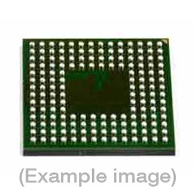
Adapters for Automated Programmers
Adapters for Manual Programmers
| 6th Gen | 7th Gen |
| FXSMR64EBGI, FXSM64EBGI, FSMR64EBGI, FSM64EBGI, FXSM64EBGC, FXSM64EBGA, FSM64EBGC, FSM64EBGA, FXASMR64EBGI, FXASM64EBGI, FASMR64EBGI, FASM64EBGI, FXASM64EBGC, FXASM64EBGA, FASM64EBGC, FASM64EBGA | FX4SMR64EBGI, FX4SM64EBGI, FXSMR64EBGI, FXSM64EBGI, FSMR64EBGI, FSM64EBGI, FXSM64EBGC, FXSM64EBGA, FSM64EBGC, FSM64EBGA, FX4ASMR64EBGI, FX4ASM64EBGI, FXASMR64EBGI, FXASM64EBGI, FASMR64EBGI, FASM64EBGI, FXASM64EBGC, FXASM64EBGA, FASM64EBGC, FASM64EBGA, LX4ASMR64EBGI (repl.), WX4ASM64EBGI (repl.) |
Adapters for Engineering Programmers
| 6th Gen | 7th Gen |
| FXSMR64EBGI, FXSM64EBGI, FSMR64EBGI, FSM64EBGI, FXSM64EBGC, FXSM64EBGA, FSM64EBGC, FSM64EBGA, FXASMR64EBGI, FXASM64EBGI, FASMR64EBGI, FASM64EBGI, FXASM64EBGC, FXASM64EBGA, FASM64EBGC, FASM64EBGA | FX4SMR64EBGI, FX4SM64EBGI, FXSMR64EBGI, FXSM64EBGI, FSMR64EBGI, FSM64EBGI, FXSM64EBGC, FXSM64EBGA, FSM64EBGC, FSM64EBGA, FX4ASMR64EBGI, FX4ASM64EBGI, FXASMR64EBGI, FXASM64EBGI, FASMR64EBGI, FASM64EBGI, FXASM64EBGC, FXASM64EBGA, FASM64EBGC, FASM64EBGA, LX4ASMR64EBGI (repl.), WX4ASM64EBGI (repl.) |
Last Updated: 05/18/2023
If the device is not yet supported by your BPM programmer (Generation), request Device Support
Note
IMPORTANT: Numonyx Axcell(R) Flash Memory. This device contains one bottom boot code segment flash die and one top boot data segment flash die. Device contains 34 128-bit Protection Registers Flash 1 PR0 through PR16 located at address range [4000000h-400010Fh] in the buffer. Example: Flash 1 PR0[0x81-0x88] is located at [4000000h-400000Fh] Flash 1 PR1[0x8A-0x91] at [4000010h-400001Fh] and so on. Flash 1 PR0[63:0] are permanently programmed by Intel with a unique number for each flash device. Flash 1 PR0[127:64] and PR1 through PR16 are one-time programmable (OTP) and available for user to program. Flash 2 PR0 through PR16 located at address range [4000110h-400021Fh] in the buffer. Example: Flash 2 PR0[0x81-0x88] is located at [4000110h-400011Fh] Flash 2 PR1[0x8A-0x91] at [4000120h-400012Fh] and so on. Flash 2 PR0[63:0] are permanently programmed by Intel with a unique number for each flash device. Flash 2 PR0[127:64] and PR1 through PR16 are one-time programmable (OTP) and available for user to program. If one or more OTP registers are programmed the range must be set to exclude the registers or the ERASE command will fail. Once programmed the user-programmable register can be locked to prevent further programming using Device > Configure menu. Once the protection register is locked the entire user segment is locked and no more user bits may be programmed. One Time Protection is available in 3 different customer ordered options: The first option-Standard OTP’ does not allow any special OTP protection of the main array. The second option-‘Simple OTP’ for each die allows up to 512KB of Main Memory OTP protection. This option pre-defines 512KB of the main array that includes the 4×32 KB parameter blocks ganged together as one block and the adjacent 3×128 KB main blocks. Please set the bit according to the main block needed to be protected under Device > Configure:
| Lock Register 0(Flash 1) | Block Protected | Bit 2 | Blocks 3:0(parameters) | Bit 3 | Block 4(main) | Bit 4 | Block 5(main) | Bit 5 | Block 6(main) | Bit 6 | Lock Bits 2-5 | Lock Register 0(Flash 2) | Block Protected | Bit 2 | Blocks 514:517(parameters) | Bit 3 | Block 513(main) | Bit 4 | Block 512(main) | Bit 5 | Block 511(main) | Bit 6 | Lock Bits 2-5 | |
|---|
| OTP Address of Flash 1(1) | Data Pattern Address | Main Array Blocks Protected | ECh | 40000D5h-40000D4h | 18:0(2) | EDh | 40000D7h-40000D6h | 34:19 | F0h | 40000DDh-40000DCh | 50:35 | F1h | 40000DFh-40000DEh | 66:51 | F4h | 40000E5h-40000E4h | 82:67 | F5h | 40000E7h-40000E6h | 98:83 | F8h | 40000EDh-40000ECh | 114:99 | F9h | 40000EFh-40000EEh | 130:115 | FCh | 40000F5h-40000F4h | 146:131 | FDh | 40000F7h-40000F6h | 162:147 | 100h | 40000FDh-40000FCh | 178:163 | 101h | 40000FFh-40000FEh | 194:179 | 104h | 4000105h-4000104h | 210:195 | 105h | 4000107h-4000106h | 226:211 | 108h | 400010Dh-400010Ch | 242:227 | 109h | 400010Fh-400010Eh | 258:243 | OTP Address of Flash 2(1) | Data Pattern Address | Main Array Blocks Protected | ECh | 40001E5h-40001E4h | 499:517(3) | EDh | 40001E7h-40001E6h | 483:498 | F0h | 40001EDh-40001ECh | 467:482 | F1h | 40001EFh-40001EEh | 451:466 | F4h | 40001F5h-40001F4h | 435:450 | F5h | 40001F7h-40001F6h | 419:434 | F8h | 40001FDh-40001FCh | 403:418 | F9h | 40001FFh-40001FEh | 387:302 | FCh | 4000205h-4000204h | 371:386 | FDh | 4000207h-4000206h | 355:370 | 100h | 400020Dh-400020Ch | 339:354 | 101h | 400020Fh-400020Eh | 323:338 | 104h | 4000215h-4000214h | 307:322 | 105h | 4000217h-4000216h | 291:306 | 108h | 400021Dh-400021Ch | 275:290 | 109h | 400021Fh-400021Eh | 259:274 | |
|---|
BPM does not sell programmable devices, nor do we program devices directly. BPM makes programmers and accessories to make programming in-house fast, easy, and profitable.
Additional information
| Manufacturer | Numonyx |
|---|---|
| Packages | BGA(64) |
| Part Number | PC48F4400P0VB02E |
| Set programming | Yes |
| Vcc(program) | 1.9 |
| Package |
