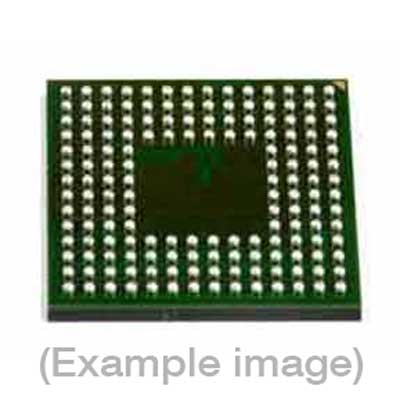
Adapters for Automated Programmers
| 9th Gen |
| LX2ASMR416BGT |
Adapters for Manual Programmers
| 9th Gen |
| LX2ASMR416BGT |
Adapters for Engineering Programmers
Last Updated: 05/18/2023
If the device is not yet supported by your BPM programmer (Generation), request Device Support
Note
IMPORTANT:
| Device Type: | Microcontroller |
| Device Size: | 8MB flash |
| Algorithm Programming Method: | Standard Software Driver v1.1.0 |
Memory Organization:
| Memory Type |
Attributes(*)
|
Included in default Range (Y/N) | DUT Physical Byte Address(hex)(if this area is selected/Activated) | BPWin Buffer Byte Address(hex) | Low and Mid address space. | R/W/E | Yes | 0000 0000 – 0001 FFFF | 0000 0000 – 0003 FFFF | UTEST Flash Memory map-OTP:Test ModeJTAG Password and Configuration Format(DCF) Records | R/W | Yes | 0020 0000 – 0020 07FF | 0040 0000 – 0040 0FFF | UTEST-Customer OTP data. | R/W | Yes | 0020 0800 – 0020 1FFF | 0040 1000 – 0040 3FFF |
| Large address space. | R/W/E | Yes | 0040 0000 – 007F FFFF | 0080 0000 – 00FF FFFF |
| Default Algorithm Range | — | — | 0000 0000 – 007F FFFF | 0000 0000 – 00FF FFFF |
* R:Read only W: One time programmable (OTP) R/W: readable and one time programmable (OTP) R/W/E: readable and rewritable if not locked. Any configurations listed under Device-Specific’ in the menu item Device-> Settings will be written to the DUT during ‘Program’ operation. Special Device Considerations: This algorithm supports verify command with CheckSum function from Standard Software Driver v1.1.0. for C55 Flash. The CheckSum function will perform a 32-bit sum over the specified flash memory range without carry which provides a rapid method for checking data integrity. UTEST-JTAG Password and PASS Password Groups as follow: Data Pattern: [0x00400010-0x0040001F]:Test Mode Disable Block Select Group A. [0x00400030-0x0040003F]:Test Mode Disable Block Select Group B. [0x00400100-0x00400103]:Test Mode Disable Override Passcode. [0x00400120-0x0040013F]:JTAG Password. [0x00400140-0x004001BF]:PASS Password Group [0-4]. [0x00400220-0x0040022F]:PLife cycle slot 2 – OEM Production. [0x00400230-0x0040023F]:Life cycle slot 3 – In Field. [0x00400240-0x0040024F]:Life cycle slot 4 – Failure Analysis. [0x00400308-0x00400FFF]:Device Configuration Format(DCF). UTEST-Device customer OTP data. Data Pattern: [0x00401000-0x00403FFF]:customer OTP data. After a successful Program + Verify operation subsequent stand alone operations may fail if the Customer Data Pattern code executes to modify the Code Flash. Serialization is not supported for this device. This algorithm do not supported JTAG password challenge. ‘
BPM does not sell programmable devices, nor do we program devices directly. BPM makes programmers and accessories to make programming in-house fast, easy, and profitable.
Additional information
| Manufacturer | NXP Semiconductors |
|---|---|
| Packages | TEPBGA(676) |
| Part Number | SPC5777CLK3MME3 |
| Set programming | Yes |
| Vcc(program) | 1.3 |
| Package |
