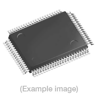
Adapters for Automated Programmers
| 7th Gen |
| FX4ASMR80LQFPU, FASMR80LQFPU, LX4ASMR80LQFPU (repl.) |
Adapters for Manual Programmers
| 7th Gen |
| FX4ASMR80LQFPU, FASMR80LQFPU, LX4ASMR80LQFPU (repl.) |
Adapters for Engineering Programmers
| 7th Gen |
| FX4ASMR80LQFPU, FASMR80LQFPU, LX4ASMR80LQFPU (repl.) |
Last Updated: 05/18/2023
If the device is not yet supported by your BPM programmer (Generation), request Device Support
Note
IMPORTANT: Algorithm support for this device selection is developed. Device samples are needed for QA testing and full release in BPWin.For information on how to obtain an expedited release of this device support please contact BPM Microsystems at:Inside Sales713–688-4600inside_sales@bpmmicro.comInformation on expected socket module support can be found our web page at: http://www.www.bpmmicro.com/find-your-device/**Please note that receipt of device samples and QA testing must be completed before socket module support can be validated.
| Device Type: | Microcontroller |
| Device Size: | 96 KByte Code Flash + 8 KByte Data Flash |
| Algorithm Programming Method: | Two-wire UART |
Memory Organization:
| Memory Type |
Attributes(*)
|
Included in default Range (Y/N) | DUT Physical Byte Address(hex)(if this area is selected/Activated) | BPWin Buffer Byte Address(hex) |
| Code Flash | R/W/E | Yes | 0000_0000 – 0001_7FFF | 0000_0000 – 0001_7FFF |
| Data Flash | R/W/E | Yes | 000F_1000 – 000F_2FFF | 000F_1000 – 000F_2FFF |
| Default Algorithm Range | — | — | 0000_0000 – 000F_2FFF | 0000_0000 – 000F_2FFF |
* R:Read only W: One time programmable (OTP) R/W: readable and one time programmable (OTP) R/W/E: readable and rewritable if not locked. Any configurations listed under Device-Specific’ in the menu item Device-> Settings will be written to the DUT during ‘Program’ operation regardless of memory range selection. Special Device Considerations:
| Option | Description |
| Security Flag | Set Bit 1 to 0 will disable Boot cluster rewrite. Set Bit 2 to 0 will disable Block Erase. Set Bit 4 to 0 will disable Program.Bits 0 3 5 6 and 7 are reserved and should be set to 1s.Bit 4 can be erased through Erase.Once bit 2 is programmed to 0 the whole chip is secured and no further operations can be performed.Once Bit 1 is programmed to 0 the boot block clusters specified are secured and no further operations can be performed. |
| 1. | Boot cluster 0 is located in Clode Flash address 00000h – 01FFFh. Boot cluster 1 is located in Clode Flash address 02000h – 03FFFh. | |
| 2. | The Security Byte can be set under Device->Configure and programmed with Secure command. | |
| 3. | Configuration options will only be programmed and verified in the Secure command. | |
| 4. | Erasing a non-blank device requires selecting the ‘Entire Device’ range under Device->Settings. | |
| 5. | This algorithm supports Firmware version V3.03 and below. | |
‘
BPM does not sell programmable devices, nor do we program devices directly. BPM makes programmers and accessories to make programming in-house fast, easy, and profitable.
Additional information
| 8-bit Bytes | 995328 |
|---|---|
| Manufacturer | Renesas |
| Packages | QFP(80) |
| Part Number | R5F100MFGFB |
| Set programming | Yes |
| Vcc(program) | 3.3 |
| Package |
