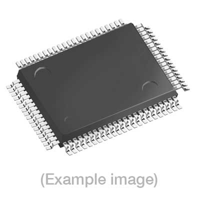
Adapters for Automated Programmers
| 8th Gen | 9th Gen |
| FVE2ASMR144QPW, FVE2ASMR144QPW | FVE2ASMR144QPW |
Adapters for Manual Programmers
| 8th Gen | 9th Gen |
| FVE2ASMR144QPW, FVE2ASMR144QPW | FVE2ASMR144QPW |
Adapters for Engineering Programmers
Last Updated: 05/18/2023
If the device is not yet supported by your BPM programmer (Generation), request Device Support
Note
IMPORTANT: [This is a custom algorithm. This algorithm has 32-bit precision in the DataFlash region.]
| Device Type: | RH850G3M CPU core Microcontroller |
| Device Size: | 2MB Code Flash + 32kB User Area + 64kB Data Flash |
| Algorithm Programming Method: | 3-Wire Serial I/O Mode. |
Memory Organization:
| Memory Type |
Attributes(*)
|
Included in default Range (Y/N) | DUT Physical Byte Address (hex)(if this area is selected/Activated) | BPWin Buffer Byte Address (hex) |
| Code Flash | R/W/E | Yes | 0000_0000 – 001F_FFFF | 0000_0000 – 001F_FFFF |
| User Area Flash | R/W/E | Yes | 0100_0000 – 0100_7FFF | 0100_0000 – 0100_7FFF |
| Data Flash () | R/W/E | Yes | FF20_0000 – FF20_FFFF | FF20_0000 – FF20_FFFF |
| Default Algorithm Range | — | — | 0000_0000 – FF20_FFFF | 0000_0000 – FF20_FFFF |
*R:Read only W: One time programmable (OTP) R/W: readable and one time programmable (OTP) R/W/E: readable and rewritable if not locked. Data Flash range is programmed & verified with 32-bit precision. Any configurations listed under Device-Specific’ in the menu item Device-> Settings will be written to the DUT during ‘Program’ operation regardless of memory range selection. Special Device Considerations:
| Option | Description |
| Security Flag | Set Bit 5 to 0 will disable Erase. Set Bit 6 to 0 will disable Program. Set Bit 7 to 0 will disable Read.Bits 4 to 0 are reserved and should be set to 1s.The Security Byte cannot be erased and once bit 5 is programmed to 0the whole chip is secured and no further operations can be performed. |
| 1. | Verification for this device is performed using the internal CRC feature of the device. | |||||||
| The Data Pattern CRC is compared and validated against the CRC value returned internally by the device. | ||||||||
| Device specifications provide details on how this CRC is calculated. | ||||||||
| 2. | The Security Flag can be set under Device->Configure and programmed with Secure command. | |||||||
| 3. | Security Byte will only be programmed and verified in the Secure command. | |||||||
| 4. | This algorithm supports Firmware version RH850 V3 or later. | |||||||
| 5. | Serialization is not supported. | |||||||
| 6. | Renesas Flash Programmer Image File (*.rpi) feature supported on Renesas R7F701421EAFB#KA0 (Custom 02) Algo.
| 7. |
Unprogrammed parts of the Data Flash will be in the erased state and readback data is in an unkown state. |
8. |
Support for .mhx file format added to program DataFlash region with ‘0xFF’ bytes where indicated by the .mhx file.a. After selecting this device the user must reload the .mhx file to correctly parse the DataFlash range.b. After the user loads a valid .mhx file the DataFlash portion of the buffer should never be modified. |
| |||
‘
BPM does not sell programmable devices, nor do we program devices directly. BPM makes programmers and accessories to make programming in-house fast, easy, and profitable.
Additional information
| 8-bit Bytes | 4280352768 |
|---|---|
| Manufacturer | Renesas |
| Packages | QFP(144) |
| Part Number | R7F701421EAFB#KA0 |
| Vcc(program) | 3.3 |
| Package |
