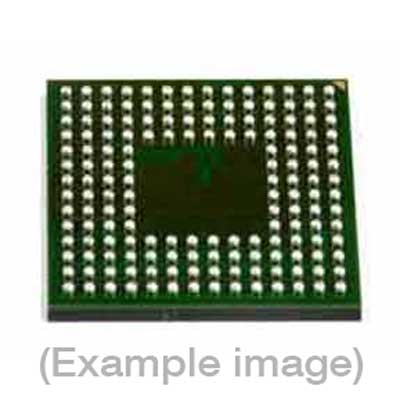
Adapters for Automated Programmers
| 8th Gen | 9th Gen |
| FVE2ASMR352BGC, FVE2ASMR352BGC | FVE2ASMR352BGC |
Adapters for Manual Programmers
| 8th Gen | 9th Gen |
| FVE2ASMR352BGC, FVE2ASMR352BGC | FVE2ASMR352BGC |
Adapters for Engineering Programmers
Last Updated: 05/18/2023
If the device is not yet supported by your BPM programmer (Generation), request Device Support
Note
IMPORTANT:
| Device Type: | V850E2M-M CPU core |
| Device Size: | 3MByte Code Flash + 32kByte Data Flash |
| Algorithm Programming Method: | 3-Wire Serial I/O Mode. |
Memory Organization:
| Memory Type |
Attributes(*)
|
Included in default Range (Y/N) | DUT Physical Byte Address(hex)(if this area is selected/Activated) | BPWin Buffer Byte Address(hex) |
| Code Flash | R/W/E | Yes | 0000_0000 – 002F_FFFF | 0000_0000 – 002F_FFFF |
| Data Flash | R/W/E | Yes | 0200_0000 – 0200_7FFF | 0200_0000 – 0200_FFFF (w/ID Tags) |
| Default Algorithm Range | — | — | 0000_0000 – 0200_7FFF | 0000_0000 – 0200_FFFF |
* R:Read only W: One time programmable (OTP) R/W: readable and one time programmable (OTP) R/W/E: readable and rewritable if not locked. Any configurations listed under Device-Specific’ in the menu item Device-> Settings will be written to the DUT during ‘Program’ operation regardless of memory range selection. Special Device Considerations:
| Bit |
Attributes and Details
|
| Bit 1 | Set Bit 1 to 0 will disable Boot cluster rewrite. Once Bit 1 is programmed to 0 the boot block clusters specified are secured and no further operations can be performed. |
| Bit 2 | Set Bit 2 to 0 will disable Block Erase. |
| Bit 3 | Set Bit 3 to 0 will disable Chip Erase. Once bit 3 is programmed to 0 the whole chip is secured and no further operations can be performed. |
| Bit 4 | Set Bit 4 to 0 will disable Program. Bit 4 can be erased through Chip Erase |
| Bit 5 | Set Bit 5 to 0 will disable Read. Bit 5 can be erased through Chip Erase |
| Bits 0 6 & 7 | Bits 0 6 & 7 are reserved and should be set to 1s. |
*The Security Byte can be set under Device->Configure and programmed with Secure command. Security for this device cannot be verified. ‘
BPM does not sell programmable devices, nor do we program devices directly. BPM makes programmers and accessories to make programming in-house fast, easy, and profitable.
Additional information
| 8-bit Bytes | 33619968 |
|---|---|
| Manufacturer | Renesas |
| Packages | BGA(352) |
| Part Number | UPD70F3532F1A9-KN7-A |
| Vcc(program) | 3.3 |
| Package |
