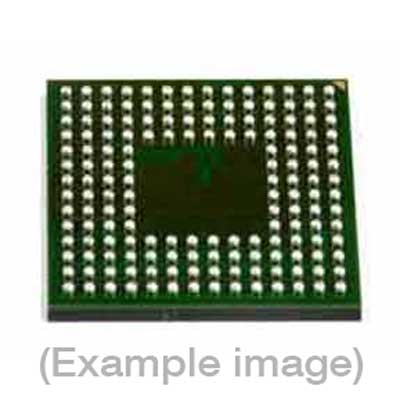
Adapters for Automated Programmers
| 9th Gen |
| FVE2ASMR352BGC |
Adapters for Manual Programmers
| 9th Gen |
| FVE2ASMR352BGC |
Adapters for Engineering Programmers
Last Updated: 05/18/2023
If the device is not yet supported by your BPM programmer (Generation), request Device Support
Note
IMPORTANT: This algorithm requires a hex data file generated via Renesas HEX Consolidation Utility (HCU).
| Device Type: | V850E2M-M CPU core |
| Device Size: | 3MByte Code Flash + 32kByte Data Flash |
| Algorithm Programming Method: | 3-Wire Serial I/O Mode. |
Memory Organization:
| Memory Type |
Attributes(*)
|
Included in default Range (Y/N) | DUT Physical Byte Address(hex)(if this area is selected/Activated) | BPWin Buffer Byte Address(hex) |
| Code Flash | R/W/E | Yes | 0000_0000 – 002F_FFFF | 0000_0000 – 002F_FFFF |
| Option Bytes | R/W | Yes | 00F0_0000 – 00F0_005F | 00F0_0000 – 00F0_005F |
| Data Flash | R/W/E | Yes | 0200_0000 – 0200_7FFF | 0200_0000 – 0200_FFFF (w/ID Tags) |
| Default Algorithm Range | — | — | 0000_0000 – 0200_7FFF | 0000_0000 – 0200_FFFF |
* R:Read only W: One time programmable (OTP) R/W: readable and one time programmable (OTP) R/W/E: readable and rewritable if not locked. Any configurations listed under ‘Device-Specific’ in the menu item Device-> Settings will be written to the DUT during ‘Program’ operation regardless of memory range selection. Special Device Considerations: For AutoRange purposes each block contains 4096 bytes. Data Pattern containing Data Flash must include valid ID Tags. Serialization is not supported. Erase function is skipped if device is blank. Erase function for a Blank secured device is not supported if chip erase is disabled. Security Bytes and Option Bytes must be erased before reprogramming. Selecting Erase will execute a chip erase on the entire device. Set OCD ID is curretly not supported. Verification for this device is performed using the internal CRC feature of the device. The Data Pattern CRC is compared and validated against the CRC value returned internally by the device. Device specifications provide details on how this CRC is calculated. Secure must be enabled to program or verify option byte and security byte. The Configuration bytes are located at Buffer addresses [F00000h-F0002Bh]. The Option Byte 0 can be set under Device->Configure and programmed with Secure command. This algorithm supports silicon version ES3.2 and below.
| Bit |
Attributes and Details
|
| Bit 0 | Set Bit 0 to 1 will disable Program. Bit 0 can be erased through Chip Erase |
| Bit 1 | Set Bit 1 to 1 will disable Block Erase. |
| Bit 2 | Set Bit 2 to 1 will disable Chip Erase. Once bit 2 is programmed to 1 the whole chip is secured and no further operations can be performed. |
| Bit 3 | Set Bit 3 to 1 will disable Read. Bit 3 can be erased through Chip Erase. Read disable disables verification of the option bytes. |
| Bit 4 | Set Bit 4 to 1 will disable Boot cluster rewrite. Once Bit 4 is programmed to 1 the boot block clusters specified are secured and no further operations can be performed. |
| Bits 5 6 & 7 | Bits 5 6 & 7 are reserved and should be set to 0. |
*The Security Byte can be set under Device->Configure and programmed with Secure command. Security for this device cannot be verified.
| Configuration Option | BPWin Buffer Byte Address (hex) | Attributes |
| Security Byte | 00F0_0000 | Readable/Writeable |
| Boot Block Cluster Last Block Number(0-127) | 00F0_0004 | Readable/Writeable |
| Flash Shield Window Start Block Number | 00F0_000C – 00F0_000D | Readable/Writeable |
| Flash Shield Window End Block number | 00F0_0010 – 00F0_0011 | Readable/Writeable |
| OCD Security ID | 00F0_0018 – 00F0_0023 | Read Only |
| Option Byte 0 – Low Bytes | 00F0_0028 – 00F0_0029 | Readable/Writeable |
| Option Byte 0 – High Bytes | 00F0_002A – 00F0_002B | Readable/Writeable |
| Option Byte 1 – 8 | 00F0_002C – 00F0_004B | Read Only |
‘
BPM does not sell programmable devices, nor do we program devices directly. BPM makes programmers and accessories to make programming in-house fast, easy, and profitable.
Additional information
| 8-bit Bytes | 33619968 |
|---|---|
| Manufacturer | Renesas |
| Packages | BGA(352) |
| Part Number | UPD70F3532F1A9-KN7-Q-A |
| Vcc(program) | 3.3 |
| Package |
