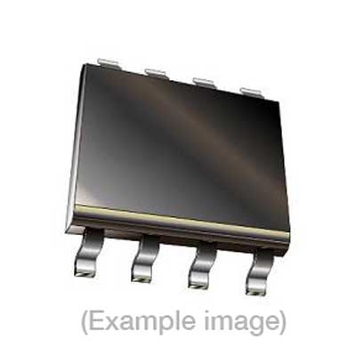
Spansion S25FS128SAGMFI100 SOIC(8) Device
Adapters for Automated Programmers
| 6th Gen | 7th Gen | 9th Gen |
| FASMR08SHL, FASM08SHL, FASMR08SHA (obs.), FASM08SHA (obs.), FASM08SG (obs.), WASM08SHA (obs.) (repl.) | FX4ASMR08SHL, FX4ASM08SHL, FASMR08SHL, FASM08SHL, FX4ASMR08SHA (obs.), FASMR08SHA (obs.), FASM08SHA (obs.), FASM08SG (obs.), LX4ASM08SHL (repl.), WX4ASMR08SHA (obs.) (repl.), WASM08SHA (obs.) (repl.) | LX4ASM08SHL, WX4ASMR08SHA (obs.), WASM08SHA (obs.) |
Adapters for Manual Programmers
| 6th Gen | 7th Gen | 9th Gen |
| FSMR08SHL, FSM08SHL, FASMR08SHL, FASM08SHL, FSMR08SHA (obs.), FSM08SHA (obs.), FSM08SG (obs.), FASMR08SHA (obs.), FASM08SHA (obs.), FASM08SG (obs.), WASM08SHA (obs.) (repl.) | FX4SMR08SHL, FX4SM08SHL, FSMR08SHL, FSM08SHL, FX4ASMR08SHL, FX4ASM08SHL, FASMR08SHL, FASM08SHL, FX4SMR08SHA (obs.), FSMR08SHA (obs.), FSM08SHA (obs.), FSM08SG (obs.), FX4ASMR08SHA (obs.), FASMR08SHA (obs.), FASM08SHA (obs.), FASM08SG (obs.), LX4ASM08SHL (repl.), WX4ASMR08SHA (obs.) (repl.), WASM08SHA (obs.) (repl.) | LX4ASM08SHL, WX4ASMR08SHA (obs.), WASM08SHA (obs.) |
Adapters for Engineering Programmers
| 6th Gen | 7th Gen |
| FSMR08SHL, FSM08SHL, FASMR08SHL, FASM08SHL, FSMR08SHA (obs.), FSM08SHA (obs.), FSM08SG (obs.), FASMR08SHA (obs.), FASM08SHA (obs.), FASM08SG (obs.), WASM08SHA (obs.) (repl.) | FX4SMR08SHL, FX4SM08SHL, FSMR08SHL, FSM08SHL, FX4ASMR08SHL, FX4ASM08SHL, FASMR08SHL, FASM08SHL, FX4SMR08SHA (obs.), FSMR08SHA (obs.), FSM08SHA (obs.), FSM08SG (obs.), FX4ASMR08SHA (obs.), FASMR08SHA (obs.), FASM08SHA (obs.), FASM08SG (obs.), LX4ASM08SHL (repl.), WX4ASMR08SHA (obs.) (repl.), WASM08SHA (obs.) (repl.) |
Last Updated: 05/18/2023
If the device is not yet supported by your BPM programmer (Generation), request Device Support
Note
IMPORTANT:
| Device Type: | Flash Memory |
| Device Size: | 256 Mbyte |
| Algorithm Programming Method: | Standard SPI |
Memory Organization:
| Memory Type |
Attributes(*)
|
Included in default Range (Y/N) | DUT Physical Byte Address(hex)(if this area is selected/Activated) | BPWin Buffer Byte Address(hex) |
| Flash Memory Array | [R/W/E] | [Yes] | [000_0000-0FF_FFFF] | [000_0000-0FF_FFFF] |
| Reserved | [R] | [No] | [000_0000-000_000F] | [100_0000-100_000F] |
| Lock Bits | [R/W] | [No] | [000_0010-000_001F] | [100_0010-100_001F] |
| OTP Region | [R/W] | [No] | [000_0020-000_03FF] | [100_0020-100_03FF] |
| Password | [R/W] | [No] | [000_0000-000_0007] | [100_0400-100_0407] |
| Default Algorithm Range | — | — | 000_0000-0FF FFFF | 000_0000-0FF FFFF |
* R:Read only W: One time programmable (OTP) R/W: readable and one time programmable (OTP) R/W/E: readable and rewritable if not locked. Any configurations listed under Device-Specific’ in the menu item Device-> Settings will be written to the DUT during ‘Program’ operation regardless of memory range selection. Special Device Considerations:
‘
BPM does not sell programmable devices, nor do we program devices directly. BPM makes programmers and accessories to make programming in-house fast, easy, and profitable.
Additional information
| 8-bit Bytes | 16778248 |
|---|---|
| Manufacturer | Spansion |
| Packages | SOIC(8) |
| Part Number | S25FS128SAGMFI100 |
| Set programming | Yes |
| Vcc(program) | 3.6 |
| Package |