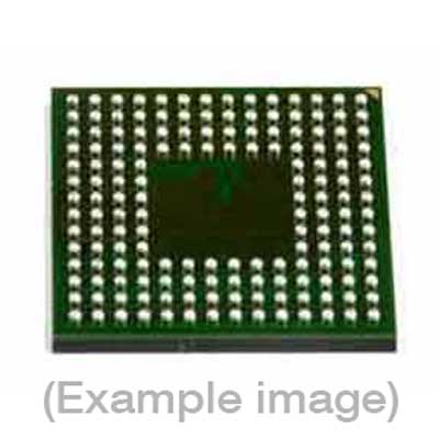
Adapters for Automated Programmers
| 6th Gen | 7th Gen |
| FXASM72SPA1, FASM72SPA1, FASM72FBG, FXASM72SPA (obs.), FASM72SPA (obs.) | FXASM72SPA1, FASM72SPA1, FASM72FBG, FXASM72SPA (obs.), FASM72SPA (obs.) |
Adapters for Manual Programmers
| 6th Gen | 7th Gen |
| FXSM72SPA1, FSM72SPA1, FSM72FBG, FXASM72SPA1, FASM72SPA1, FASM72FBG, FXSM72SPA (obs.), FSM72SPA (obs.), FXASM72SPA (obs.), FASM72SPA (obs.) | FXSM72SPA1, FSM72SPA1, FSM72FBG, FXASM72SPA1, FASM72SPA1, FASM72FBG, FXSM72SPA (obs.), FSM72SPA (obs.), FXASM72SPA (obs.), FASM72SPA (obs.) |
Adapters for Engineering Programmers
| 6th Gen | 7th Gen |
| FXSM72SPA1, FSM72SPA1, FSM72FBG, FXASM72SPA1, FASM72SPA1, FASM72FBG, FXSM72SPA (obs.), FSM72SPA (obs.), FXASM72SPA (obs.), FASM72SPA (obs.) | FXSM72SPA1, FSM72SPA1, FSM72FBG, FXASM72SPA1, FASM72SPA1, FASM72FBG, FXSM72SPA (obs.), FSM72SPA (obs.), FXASM72SPA (obs.), FASM72SPA (obs.) |
Last Updated: 05/18/2023
If the device is not yet supported by your BPM programmer (Generation), request Device Support
Note
IMPORTANT: 32Mbit Flash Memory.The device has a 64-bit unique device number which is pre-programmed by the manufacturerand cannot be modified. All the 64 bits will be read at buffer locations 800000h-800007h.These bits are ignored during Compare and Verify operations.The 128 bits of User Programmable OTP cells can be modified and are located at bufferlocations 800008h-800017h.If the OTP Data Protection Bit is set further Program of the User Programmable OTP cells(Buffer locations 800008h-800017h) will fail. If the OTP cells are not blankthey have to be excluded from ERASE/PROGRAM operations.
BPM does not sell programmable devices, nor do we program devices directly. BPM makes programmers and accessories to make programming in-house fast, easy, and profitable.
Additional information
| Manufacturer | STMicroelectronics |
|---|---|
| Packages | BGA(66) |
| Part Number | M36W832TE-ZA |
| Set programming | Yes |
| Vcc(program) | 3 |
| Package |
