by Scott Bronstad | Aug 3, 2017 | Flash, Technology, White Papers
How to Maximize Speed, Quality, and Cost Savings
Abstract
Exceptional products start with exceptional programming. Mass programming is one of the important stages in the final product build and release.
This white paper shares information to help engineers involved in the industry of eMMC device programming. It summarizes the basic specification that all eMMC devices follow including device architecture, bus protocols, modes, data read/write, and production state awareness.
The white paper also lists the criteria decision-makers should consider when evaluating the effectiveness of their Universal Programming equipment. The quality and efficiency of programming equipment affect the quality and cost of the final product as well as time to market.
Introduction
Over the past decade, the demand for high-density, nonvolatile memories with a small footprint has increased dramatically. Two of the most popular markets driving this demand are handheld devices and automotive. Demand for handheld devices continues to drive the research for high-density, low power, low-cost, high-speed, nonvolatile memories while maintaining a small footprint. NAND-type flash memory is the perfect match for such a market. The increased consumer demand for high-tech features in automobiles, such as infotainment systems, is also a big driver of demand for high-density NAND-based devices.
Flash memory is a solid-state, nonvolatile storage medium that can be electrically erased and reprogrammed. There are two types of flash memory, NAND and NOR, named after the NAND and NOR logic gates. NAND flash memory was introduced by Toshiba scientists in 1987 [1] and can be written and read in blocks. NAND flash memory was not fully utilized until recently due to its low reliability. Early NAND flash experienced bit flips, the possibility that some programmed bits read back as zero while previously programmed bits read as one, or vice versa. Bit flips introduced bad blocks over the service life of the device. With the advances in research in Error Correction Codes (ECC) [2][6][7], along with implementing new Bad Block Management (BBM) schemes [3][7], engineers were able to better detect and correct bit flips. This increased the appeal of NAND flash memory and allowed it to dominate over its more expensive rival, NOR flash memory.
The inevitable use of ECC and BBM schemes with “RAW” NAND devices leads to increased complexity when handling these devices. To avoid such difficulties, and reduce the design and time to market cost, the trend shifted to the use of “managed NAND devices”. The typical architecture of any managed NAND device includes a raw NAND memory, which is the main storage media, plus a microcontroller [5]. The microcontroller acts as the interface between the host and the raw NAND memory. It does all management tasks such as bad block management, error detection, and correction, wear leveling, and more. This helps hide the complexity of these heavy lifting tasks and frees the host (and hence the designer) to focus on application-specific tasks. Furthermore, both customers and programming houses do not need to research and provide details (and sometimes example codes) for specific ECC or BBM schemes. These are many times not easy to obtain and are IP protected. Examples of managed NAND devices include Solid State Drives (SSD), Universal Flash Storage (UFS), Secure Digital (SD) cards, and Embedded Multimedia Card (eMMC) devices.
The focus of this paper is on eMMC devices. It begins with a brief overview of the eMMC device architecture, followed by sections explaining different protocols, speed modes, and write modes supported by these devices. A section discusses the new specifications and “production state awareness” feature introduced in recent JEDEC specifications version 5.0 and later. The paper concludes with the top five tips programming centers and decision-makers should consider when purchasing high-quality programmers for programming eMMC devices.
eMMC Architecture
Embedded Multimedia Card (eMMC) devices follow a standard prepared by JEDEC and the MMC Association. This standard, widely known as JEDEC specs, defines the eMMC electrical interface and its environment and handling [4].
Figure 1 provides an overview of the eMMC system and the interaction between the host and device controller. The eMMC communication protocol may use up to 11-signal bus (clock, command, data strobe, and 1, 4, or 8 data buses). [4]
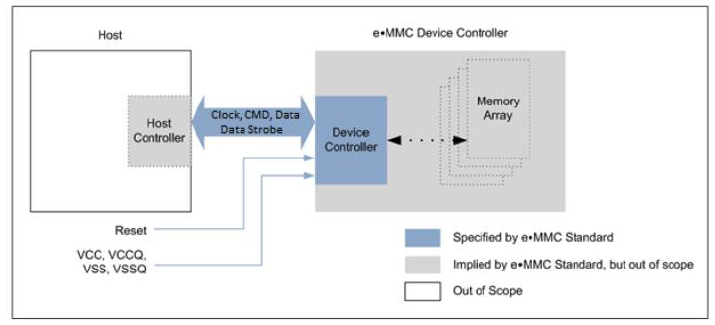
Figure 1. eMMC System Overview [4]
Figure 2 provides an example of partitions and user data area configuration. Upon shipping from the factory, the eMMC device consists of a user data area to store data, two boot area partitions for booting (Boot Area Partition 1 and Boot Area Partition 2), and Replay Protected Memory Block Area Partition (RPMB) to manage data in an authenticated and replay protected manner. The size of the boot area partitions and the RPMB areas are defined as multiple of 128 KB.
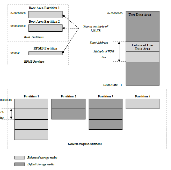
Figure 2. Example of partitions and user data area configuration [4]
To achieve high densities while maintaining a small footprint and lower cost per unit, NAND flash can be built using multi-level cell (MLC) flash memory. In MLC, a memory cell can store more than 1 bit. This normally creates negative effects on the chip lifetime since the risk of more bit flips could occur and decrease the number of Program/Erase cycles before the cell fails [6]. Since the boot area partitions and RPMB area are designed to hold sensitive data, these are shipped from factories in an enhanced state, also known as single-level cells (SLC). If needed, the user data area can later be enhanced. Moreover, up to four General Purpose partitions can be created, and the size and state of these areas can be adjusted by writing to a register called Extended Device-Specific Data (ECSD) register.
Bus Protocol
As described in the JEDEC specification [4], the communication between the host and the device follows a message-based bus protocol. One of the tokens described below represents each message:
- Command: a command token starts operation and sends serially from the host to device on the CMD line
- Response: the device sends a response token serially to the host as an answer to a previously received command on the CMD line
- Data: the data lines transfer data from the device to the host or vice versa. The data bus may be set to 1(DAT0), 4(DAT0-DAT3), or 8(DAT0-DAT7)
Each token is preceded by a start bit (‘0’) and succeeded by an end bit (‘1’). Cyclic redundancy check (CRC) follows the data in each token.
Speed Mode Advancements
The industry has seen significant improvements in the data transfer speeds supported by eMMC devices. Figure 3 summarizes a comparison of the advancements in speed modes.
Single Data Rate (SDR)
Legacy eMMC devices support a 0-26 MHz clock speed with a maximum data transfer of 26 MB/s. They use the Single Data Rate (SDR) mode to transfer data. In this mode, a single bit can be transferred on each data line per clock cycle. Later eMMC devices support a clock speed of 0-52 MHz.
Dual Data Rate (DDR)
The 0-52 MHz eMMC devices supported the legacy SDR mode as well as a newer transfer mode introduced by JEDEC version 4.4 called Dual Data Rate (DDR). DDR mode allows the transfer of two bits on each data line per clock cycle, one per clock edge. This helps achieve a transfer rate of up to 104 MB/s. In this mode, two CRCs need to be sent after each block of data, one for bytes with an odd number and another for bytes with an even number. This totals 32 bytes, instead of 16 bytes in SDR mode, for an 8-bit data bus.
HS200
JEDEC version 4.5 introduced support for even faster clock speeds of up to 200 MHz (high-speed HS200). The maximum transfer rate for this mode is 200 MB/s.
Most recently, JEDEC version 5.0 introduced a DDR version of the HS200, known as HS400. The goal of HS400 mode is to achieve maximum data transfer to 400 MB/s (Note: that goal has been realized as of 2021).
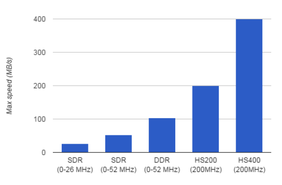
Figure 3. Speed Mode Advancements
It is worth noting that the above speeds do not take into account the overhead of command transfers and the time taken by the device to physically write a block of data to the internal memory or prepare a block of data to be sent to the host during read operation.
Data Read/Write
The JEDEC specification defines different data read/write commands for use with eMMC.
- The single block read/write – the host reads/writes a single block after issuing a “single block read/write command”
- Pre-defined multiple blocks read/write – the host sets the number of blocks to be read/written followed by the multiple blocks read/write command
- Open-ended multiple blocks read/write – the host continues to read/write blocks of data until it issues a stop transmission command
During the read operation, the device sends CRC after each 512 data bytes. In a similar manner, the host sends the CRC after 512 data bytes. If the CRC is correct, then the device sends back a positive CRC status “010b” to the host. Otherwise, it sends back a negative CRC status “101b” and ignores the data sent by the host. Before writing new data to any sector, the device erases the old data.
As described above, the CRC of the customer raw data file to be programmed into the device needs to be calculated. One option is to reformat the data file by embedding the CRC values after each sector. Most programmers have a tool that can perform this operation offline.
Production State Awareness
JEDEC version 5.0 introduces “Production State Awareness” to help avoid possible data corruption during soldering. Activate the Production State Awareness by setting a field in the extended CSD register before programming the part. Only a predefined part of the whole device’s available space can be supported by this feature.
5 Tips When Programming eMMC
Exceptional products start with exceptional programming. This section outlines the top five considerations manufacturers and programming centers need to look for that affect resource utilization, net throughput, and quality of programming.
1. Use HS400 Mode for High Throughput
Make sure your device programmer supports HS400 mode. To achieve high throughput, programmers need to support the highest possible speed mode currently supported by the device. JEDEC recommends HS400 mode when programming eMMC devices to achieve the highest possible programming speed. Don’t compensate for slower programming times by buying more sockets. More sockets mean higher purchasing costs, more time spent teaching, and higher maintenance costs. Faster programming times allow for fewer sockets, which creates a huge multiplier effect of time and resource savings from teaching and programming to purchasing and maintenance.
2. Ensure Clean Signal Quality for High Yield
It is critical to follow programming specifications to ensure the quality of the final product. One of the signals that have crucial timing constraints in high-speed mode is the clock signal. According to JEDEC, when programming eMMC in HS400 mode the minimum pulse width must be 2.2 ns and the minimum slew rate must be 1.125 V/ns. These constraints must be maintained to achieve the highest possible speed, even if a clock period of 5 ns is used. Make sure all signals generated by your programmer follow the specification for the device. As an example, the high accuracy of the clock generated by the programmer in Figure 4 helps achieve the target transfer at a rate of 2.5 ns per byte, which puts it at the device’s limits.
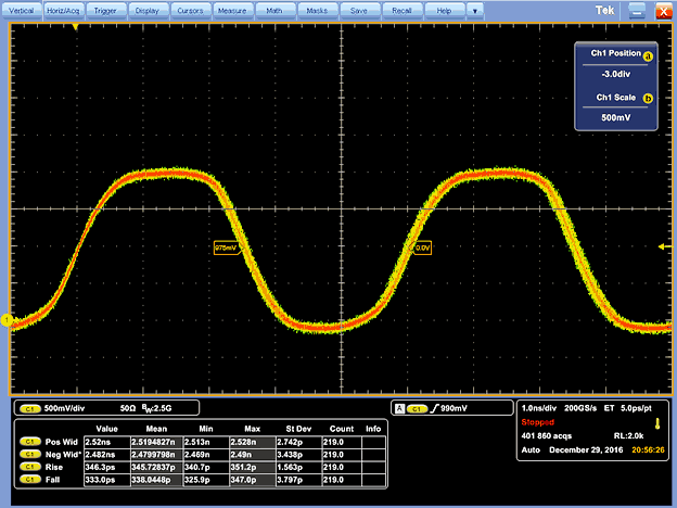
Figure 4. BPM 9th Gen Clock in HS400 Mode
3. Purchase Adaptable Socket Modules for Cost Savings
Find a partner who gives you the ability to use existing socket modules for new eMMC programming instead of requiring the purchase of new socket modules. This future-thinking partner will help you smartly manage your budget. Make sure socket modules that support DDR mode also support HS400 mode, so you have high programming flexibility and keep overall costs low.
4. Invest in Automated Programmers for High Volume
To achieve high volume production in a short amount of time, consider purchasing automated programmers. High-density devices like eMMC take a longer time to program, so investing in an automated programmer allows you to increase machine utilization and maximize throughput. Look for an automated programmer equipped with a high accuracy robotic arm and cameras to ensure both accurate and careful handling of thin eMMC devices as well as other CSP devices. This will improve the speed and accuracy of handling devices during the programming process. Some automated programmers are equipped with 3D inspection systems and laser marking systems.
5. One Programmer To Rule Them All
Invest in a device programmer that supports eMMC devices as well as other types of devices. This will quickly save you time and money. A programmer that supports a high mix of devices gives you the flexibility to program different devices on a single machine. This reduces the machine idle time and setup time between different jobs since there is no need to swap programmers for different devices. In addition, there is a reduction in maintenance and training time, since you only need to train staff on operating and maintaining one machine. Finally, there are cost savings since one universal programmer will be enough to support most, if not all, of your devices. Make the decision to add additional programmers based on capacity, not device support limitations.
Summary
This paper shared knowledge about eMMC devices and programming best practices benefitting both engineers as well as decision-makers working in the industry of eMMC device programming.
The paper briefly explained the basic device specification that all eMMC devices follow: such as device architecture, protocols, speeds modes, and read/write modes.
The paper concludes with the top five characteristics to look for when purchasing an efficient eMMC programmer to maximize quality, throughput, and cost savings:
- Ensure your programmer supports the highest possible speed mode (HS400 at time of writing this paper)
- Ensure your programmer produces clean signal integrity
- Ensure socket modules support DDR mode and HS400 mode
- Invest in automated programmers to maximize volume
- Ensure your programmer supports a high mix of devices
Download PDF Here
References
[1] S. Aritome, Kawasaki, R. Shirota, G. Hemink, T. Endoh, F. Masuoka, “Reliability issues of flash memory cells,” Proceedings of the IEEE ( Volume: 81, Issue: 5, May 1993 ).
[2] Affeldt, R., Garrigue, J., “Formalization of error-correcting codes: from hamming to modern coding theory.” In: Urban, C., Zhang, X. (eds.) ITP 2015. LNCS, vol. 9236, pp. 17–33. Springer, Heidelberg (2015). doi:10.1007/978-3-319-22102-12 4.
[3] Priyanka P. Ankolekar, Roger Isaac, and Jonathan W. Bredow, “Independent bad block management for mass storage flash memory arrays”, IEEE Transactions on Device and Materials Reliability (Volume: 10, Issue: 1, March 2010).
[4] Jedec Solid-state technology association, “Embedded Multi-Media Card (eMMC) Electrical Standard (5.1),” [https://www.jedec.org/standards-documents/docs/jesd84-b51]. http://www.jedec.org/standards-documents/results/jesd84-b51, February 2015.
[5] Sandisk, “Design Considerations for SD™ Cards and e.MMC Products”, [https://link.sandisk.com/content/dam/customer-portal/en_us/external/public/cps/collaterals/white_paper/white_paper_design_considerations_v1_0.pdf], 2015.
[6] D. Allred, G. Agarwal, “Software and hardware design challenges due to the dynamic raw NAND market”, EE Times, 2011.
[7] STMicroelectronics, “Bad block management in NAND flash memories” EET Asia, 2014.
[8] Micron, “Bad Block Management in NAND Flash Memory” Technical note TN-29-59, https://www.micron.com/~/media/documents/products/technical-note/nand-flash/tn2959_bbm_in_nand_flash.pdf, 2011.

by Scott Bronstad | Jan 12, 2015 | Announcements, New Product, News, Technology
BPM Microsystems announces double data rate (DDR) support for eMMC flash memories on 8th Generation programmers. The 8th Generation programmers already featured the fastest programming and verification times of any universal programmers. This new feature doubles the rate at which data is transferred into and out of the device during programming and verification by transferring a word of data to or from the device on both the rising and falling clock edges.
“Our automotive customers’ programming enormous data files will get an immediate increase in productivity by using DDR,” said William White, CEO of BPM Microsystems. “The programmers we are shipping today are now more than 1,000,000 times faster than the original EP-1 programmer we shipped 30 years ago.”
“The Vector Engine BitBlast DDR Mode Support is just the latest example of how the advanced Vector Engine design sets us apart from the competition. The Vector Engine continues to evolve and adapt to new requirements keeping our users up to date even as their requirements change.”
As an example of the performance that can be achieved with this new feature, 2800 and 3800MK2 programmers are now a staggering 105% faster than the closest competitor on the SanDisk SDIN8DE4-32G. The BPM programmer will perform a Program and Verify operation in 1403 seconds when programming 29GB of random data compared to 2880 seconds for the Flash Core III according to Data I/O’s website. The 3800MK2 will program and verify this device at a rate of 1190 GB/hour, enabling economic programming of enormous data patterns used in today’s automotive electronics.
By decreasing programming times, BPM has enabled customers with the 3800MK2 to achieve the devices per hour similar to competitive machines that are more than twice the footprint. In addition to the improved cost per device, the faster programming times mean that when using High Insertion Count Sockets (HIC Sockets), which can have lifetimes of up to 1 million insertions, customers only have to buy half as many sockets to get the same throughput in devices per hour. Such reductions can potentially save hundreds of thousands of dollars over the life of a machine.
All users of the 8th generation programmers that are under software contracts are eligible for a free automatic firmware update that will enable this new feature automatically when the BPWin software is updated.
Established in 1985, BPM Microsystems is known for its long history of disruptive innovation including the first universal programmer with socket modules, the first concurrent programmer, the first automated programming system with vision centering, the first flash programmer with Vector Engine and DDR and the first high-yield CSP programming system. BPM presently leads the programming industry with automated programming of CSP devices, fast programming times, rapid support for complex integrated circuits and productivity.